Product Features
•This system offers high precision, excellent stability, and flexible expandability, making it suitable for laboratory testing.
•Manual wafer replacement supports 8-12 inch wafers, accommodating different on-site requirements and providing versatility.
•Supports FAU and grating vertical coupling (Grating Coupling) and O-O optical testing.
•Supports testing parameters for coupling loss (dB/cm) and coupling efficiency (%).
•Utilizes a high-precision coupling controller with full closed-loop control and hardware synchronization, optimizing coupling algorithms to enhance accuracy and speed.
•Features image-assisted functionality for more convenient operation during the testing process, with rapid calibration and accurate initial positioning.
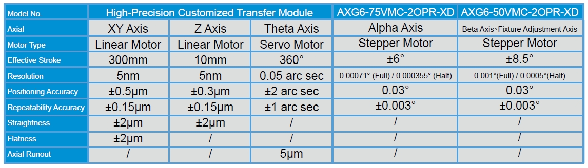
•The high-precision linear transfer stage offers repeatability accuracy 0.15 μm, meeting current industry requirements for optical coupling.
•The fixture is equipped with a high-precision height gauge to ensure consistent alignment of the incident optical fiber end face to the wafer surface, minimizing inconsistencies in coupling results and avoiding collision risks.
◎ Optical path coupling inspection in silicon photonics wafer testing.
Optical path coupling is a process in silicon photonics wafer inspection where optical fibers are aligned with the optical paths on the wafer to facilitate subsequent spectral analysis and characterization of the optical paths.
※For detailed specifications, please refer to the catalog available in the download section on the official website.
Click image link
Click image link
Click image link
